Menu:
Master’s Thesis: "A Low Input Voltage Energy Harvesting Charge Pump with Load-Adaptive Pumping Frequency"
Description
For my Master’s degree in Electrical Engineering at Washington State University, I designed a low voltage charge pump for energy harvesting applications. The charge pump is a fully integrated circuit that boosts a 300mV - 800mV output voltage from ambient energy harvesters (such as piezoelectric generators or solar cells) to a 1.2V - 3.2V voltage that can be used to power digital and analog circuitry. The charge pump uses a novel topology that addresses the challenges of operating over a wide range of input voltages and allows it to maintain high efficiency at heavy and light loading conditions.
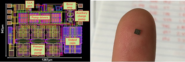
Left: Full charge pump layout. Right: Fabricated charge pump IC.
I designed the full circuit at the MOSFET level, simulated the performance using Cadence, and completed the full chip layout including DRC and LVS checks. I submitted the chip for fabrication, and performed test measurements to gauge its functionality and efficiency. I wrote a short paper discussing the charge pump topology and performance, and it is pending submission to the IEEE Transcations on Circuits and Systems journal.
I utilized excellent time management skills to complete this thesis project over the course of a year while working full time at Schweitzer Engineering Laboratories. It took grit and determination to push this project through to completion, and I am proud of the hard work I put in to it.
My full thesis can be viewed at the WSU Online Dissertation Library.
Project Takeaways
My thesis project significantly increased my knowledge of chip design and my understanding of integrated circuits. I also gained experience in the following areas:
- Switched-capacitor power supply design
- Understanding of MOSFET regions of operation, switching loss, parasitics, and SPICE models
- Design of extremely low-power oscillator and amplifier circuits
- MOSFET circuit design, schematic entry, library management, and layout using Cadence software
- Simulation of MOSFET circuit performance over statistical variations and thermal corners
- Start-to-finish layout of full silicon chip in 0.18um process:
- Layout floor planning and routing connections between sub-blocks
- Understanding and addressing design rules
- Grounding techniques and guard ring implementation to reduce switching noise
- Test measurement techniques for microelectronic circuits
- Researching journal publications and innovating on state-of-the-art circuit concepts
- Authoring technical papers
Details
Summary
The charge pump implements a load-adaptive pumping frequency scheme to achieve high-efficiency operation over a wide range of input voltage and output loading conditions. The charge pump frequency adapts to the size of the load at the output: if the load is large, the pumping frequency increases to transfer more current to the output, and if the load is small, the pumping frequency decreases to reduce switching loss while still maintaining the desired output voltage. A block diagram of the load-adaptive charge pump is shown below.
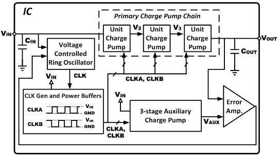
Block diagram of the load-adaptive charge pump IC
Theory of operation
Charge is transferred from the input to the output capacitor through a three-stage charge pump that is driven by large clock buffers. In ideal steady-state operation, Vout = 4*Vin. However, Vout will vary between Vin to 4*Vin depending on the load condition and the pumping frequency. The output of the auxiliary charge pump is also Vaux = 4*Vin. Vaux consistently remains close to 4*Vin because the output of the auxiliary charge pump is not connected to a load. Thus, Vaux is used as a reference voltage that is compared to Vout. Vaux and Vout are fed to the error amplifier, which generates a DC bias voltage (Vbias) ranging from 0.2*Vin to Vin. The larger the difference between Vaux and Vout, the higher Vbias is. The bias voltage is routed back to a voltage controlled oscillator (VCO), whose frequency is linearly dependent on Vbias when Vbias is in the range of 0.2*Vin to Vin. The variable clock frequency generated by the VCO is fed to the CLK generator circuit, which creates two anti-phase non-overlapping clock signals, CLKA and CLKB, which switch between 0V and Vin. CLKA and CLKB are driven by large power buffers, these buffers drive the pumping current for the primary charge pump and the auxiliary charge pump.When the output load is increased, the following sequence occurs:
- Vout drops in response to the increased load, while Vaux remains constant
- Vbias increases due to the increased difference between Vaux and Vout
- CLK frequency increases as Vbias increases
- Increased pumping frequency causes more current to be delivered to the output, increasing Vout closer to the ideal output voltage
Thus, the charge pump achieves its goal of lowering the pumping frequency at light loading conditions to reduce switching, and increasing the pumping frequency at heavy loading conditions to maintain output voltage. It also allows it to have a consistent pumping frequency over a wide range of input voltages.
Sub-circuits
These are some of the unique sub-circuits I designed for the charge pump.
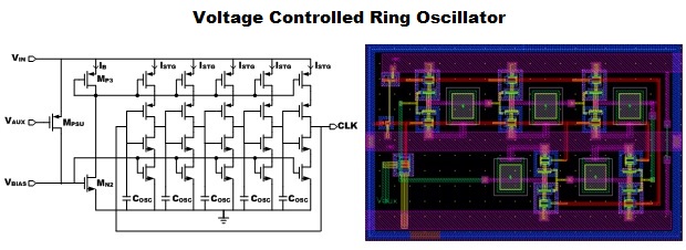
The VCO is implemented using a five stage current-starved ring oscillator. Vbias sets the amount of current that can flow through the upper PMOS and lower NMOS FETs, which directly controls the oscillation frequency. As Vbias increases, the oscillation frequency increases.
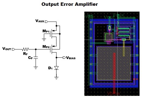
The output error amplifier compares the Vaux to Vout to generate a bias voltage, Vbias. It is a common-source amplifier with a long-channel PMOS (Mp1) used for source degeneration and a diode-connected NMOS (Mn1) as the load. If Vaux is fixed and Vout decreases, more current flows through the amplifer, increasing the voltage across D1 (Vbias).
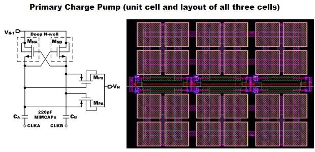
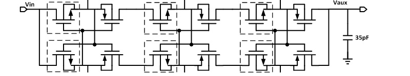
The primary charge pump chain consists of three unit cells connected back-to-back. Each stage doubles the voltage of the previous stage. The charge pump uses a dual-phase topology, where the boosted voltage of one phase is used to turn on the conducting switches of the other phase, improving conductance and allowing the charge pump to operate better at subthreshold input voltages.
Simulation results
After completing the charge pump design and layout, I extracted the layout parasitics to perform post-layout simulations of overall performance for various input voltage and loading conditions. The simulations show that charge pump works over an input voltage range of 200mV - 800mV, has a peak efficiency of 64.84% at Vin = 500mV for an output load of 200kΩ, and can produce up to 1.83mW of power with at Vin = 800mV.
A transient simulation of the charge pump’s response when the output load changes from 500kΩ to 50kΩ is shown below.
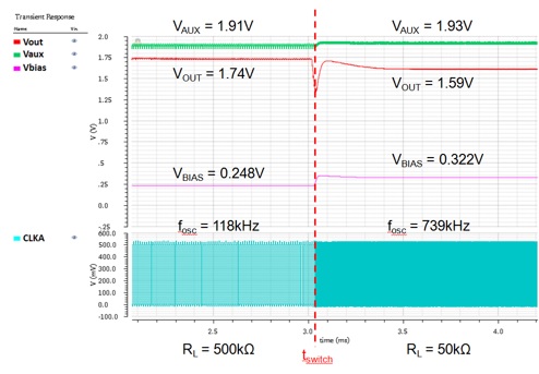
Charge pump response to sudden change in load
Initially, the output load is light, so the pumping frequency is kept low to reduce switching loss and improve efficiency. When the load increases, the Vout begins to decrease, causing Vbias to rise, which in turn causes the pumping frequency to increase. This causes more current to be transferred to the output, so the output voltage is maintained. Compared to a fixed-frequency charge pump, efficiency is improved by over 30% at light loading conditions for an input voltage of 500mV.
Test measurements
The charge pump was implemented in the TowerJazz SBC13HX 0.18um technology process, and submitted to TowerJazz for fabrication. When the fabricated chip arrived, I worked with another WSU grad student to set it up in a test measurement fixture. A picture of the setup is shown below.
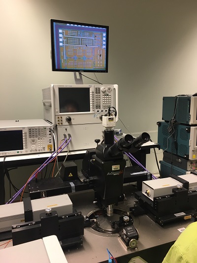
Test fixture setup for the charge pump IC. The physical layout of the IC (as seen by the microscope) is shown on the monitor above the station.
I connected a precision voltage source and a variable load to the charge pump, and measured the input current, bias voltage, and pumping frequency at different levels of input voltage and output load. Generally, the measured performance was worse than the simulated performance: the minimum input voltage the charge pump could operate at was 350mV rather than 200mV, and the peak efficiency was 59.77%. However, the charge pump still successfully adapted its pumping frequency in response to changes in load. The efficiency for an input voltage of 500mV and an output load of 500kΩ is improved 14% over that of a fixed-frequency charge pump.